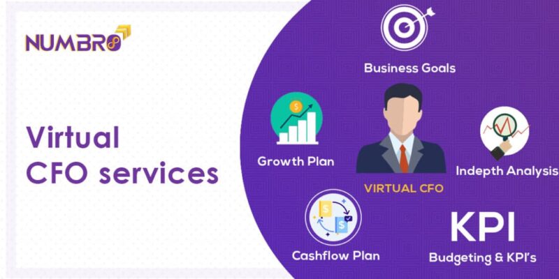
Semiconductor Ecosystem Market

Global Semiconductor Value Chain

The global semiconductor ecosystem is a marvel of complexity and interdependence. You have fabless chip design houses in India and the US, Intellectual Property (IP) licensors in the UK, wafer fabrication giants in Taiwan and Korea, and assembly and test units spread across Southeast Asia. We are now witnessing a deliberate, policy driven effort to rebalance this ecosystem. For Indian stakeholders, the question is no longer just about design services. It is about moving up the value chain toward fabless product ownership, ATMP (Assembly, Testing, Marking, and Packaging) facilities, and eventually, commercial wafer fabrication.

What Numbro covers:

Global capacity mapping across the value chain nodes: EDA tools, Wafer Fab Equipment (WFE), Foundry services, and Outsourced Semiconductor Assembly and Test (OSAT). India specific supply chain mapping of domestic players in VLSI design and the emerging compound semiconductor ecosystem (GaN/SiC). Investment landscape analysis of PLI scheme disbursements and FDI trends in electronics manufacturing. Geopolitical risk assessment of Taiwan Strait contingencies and export control regimes (Wassenaar Arrangement).

For more details, Fill this form